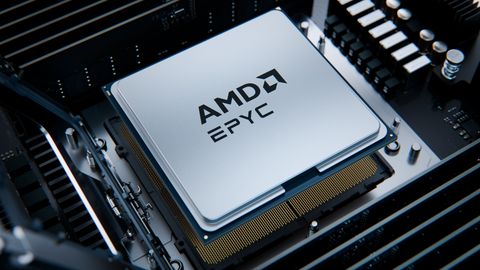
Venice-X utilizes the SP7 socket infrastructure, delivering a massive performance leap through a combination of high-density stacked SRAM and a top-tier 5.3 GHz boost frequency that overcomes the historical clock-speed penalties of previous X-series parts. The platform introduces native PCIe 6.0 support alongside a full 16-channel memory architecture, yielding nearly four times the per-socket memory bandwidth of older generations while operating within an estimated TDP range of 400W to 600W.
For enterprise buyers and large-scale HPC deployments, the elimination of the traditional frequency-versus-cache trade-off means workloads bound by both instruction-per-cycle latency and memory capacity will see immediate efficiency gains. Exact base clocks, full SKU lineups, and pricing remain unconfirmed as AMD prepares for its late-next-year rollout.